


Domestic chip breakthrough, Changdian Technology 4nm small chip to achieve mass production


Recently, China's largest and the world's third largest packaging and testing company Changdian Technology announced that the XDFOI Chiplet process has achieved a breakthrough, and began to gradually enter the stable mass production stage, synchronised to achieve the international customers 4nm node multi-chip system integration packaging product shipments, the largest package body area of about 1500mm2 system level packaging. The company developed a series of high-density multi-dimensional heterogeneous integration process can be in a limited area, to achieve high-density process integration, so that the chip package size is smaller, and stronger performance.
As we all know, the domestic industrialisation started late, in some advanced equipment and technology lags behind the West and other advanced countries, especially in the field of chip manufacturing, EUV lithography is the key to limit the development of advanced process chips in China. However, when chip manufacturing into the 3nm process, Moore's Law is increasingly difficult to break through, coupled with fierce competition in semiconductor equipment technology, lithography and other equipment prices and manufacturing costs are rapidly soaring, so that the industry is forced to look for new alternative technologies, small chips is one of the important direction, but also one of the important technological path for China's market to change lanes and overtake.
Small chip is a chip "modular" design methodology, but also a heterogeneous integration of packaging technology. To put it simply, small chips can integrate chips with different process nodes, different functions, and even different materials, like building blocks, through advanced packaging technology to form a system-on-chip (SoC) to balance the performance and cost of chip computing. Compared with the traditional SoC programme, the small chip model has three advantages: design flexibility, low cost and short time-to-market. At present, TSMC, Qualcomm and other semiconductor companies, Google, Microsoft and other IT giants, including 10 companies have launched extensive co-operation on small chip technology, open universal small chip interconnection standards, but also set up an industry alliance.
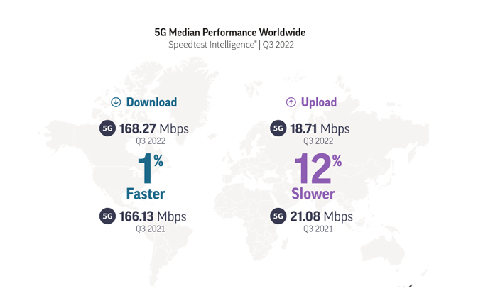
The 4 nm packaging technology of Changdian Technology, compared with the traditional 3 nm process technology, will effectively improve the density of the chip and greatly reduce the demand for chip processes. At the same time, Changdian Technology has also developed three high-density integration solutions, namely, 2D, 2.5D and 3D chiplets, of which the 2D solution adopts a special process to solve the problem of internal stress in the chip, while the 2.5D solution uses a special processing method to solve the signal integrity problem. According to the report, Changdian Technology will give full play to the technical advantages of the XDFOI Chiplet process and apply it in high-performance computing, artificial intelligence, 5G, automotive electronics and other fields to provide downstream customers with finished chip manufacturing solutions with thinner and lighter profiles, faster data transmission rates and lower power loss.
Recently, China's largest and the world's third largest packaging and testing company Changdian Technology announced that the XDFOI Chiplet process has achieved a breakthrough, and began to gradually enter the stable mass production stage, synchronised to achieve the international customers 4nm node multi-chip system integration packaging product shipments, the largest package body area of about 1500mm2 system level packaging. The company developed a series of high-density multi-dimensional heterogeneous integration process can be in a limited area, to achieve high-density process integration, so that the chip package size is smaller, and stronger performance.
As we all know, the domestic industrialisation started late, in some advanced equipment and technology lags behind the West and other advanced countries, especially in the field of chip manufacturing, EUV lithography is the key to limit the development of advanced process chips in China. However, when chip manufacturing into the 3nm process, Moore's Law is increasingly difficult to break through, coupled with fierce competition in semiconductor equipment technology, lithography and other equipment prices and manufacturing costs are rapidly soaring, so that the industry is forced to look for new alternative technologies, small chips is one of the important direction, but also one of the important technological path for China's market to change lanes and overtake.
Small chip is a chip "modular" design methodology, but also a heterogeneous integration of packaging technology. To put it simply, small chips can integrate chips with different process nodes, different functions, and even different materials, like building blocks, through advanced packaging technology to form a system-on-chip (SoC) to balance the performance and cost of chip computing. Compared with the traditional SoC programme, the small chip model has three advantages: design flexibility, low cost and short time-to-market. At present, TSMC, Qualcomm and other semiconductor companies, Google, Microsoft and other IT giants, including 10 companies have launched extensive co-operation on small chip technology, open universal small chip interconnection standards, but also set up an industry alliance.
The 4 nm packaging technology of Changdian Technology, compared with the traditional 3 nm process technology, will effectively improve the density of the chip and greatly reduce the demand for chip processes. At the same time, Changdian Technology has also developed three high-density integration solutions, namely, 2D, 2.5D and 3D chiplets, of which the 2D solution adopts a special process to solve the problem of internal stress in the chip, while the 2.5D solution uses a special processing method to solve the signal integrity problem. According to the report, Changdian Technology will give full play to the technical advantages of the XDFOI Chiplet process and apply it in high-performance computing, artificial intelligence, 5G, automotive electronics and other fields to provide downstream customers with finished chip manufacturing solutions with thinner and lighter profiles, faster data transmission rates and lower power loss.


