


Semiconductor
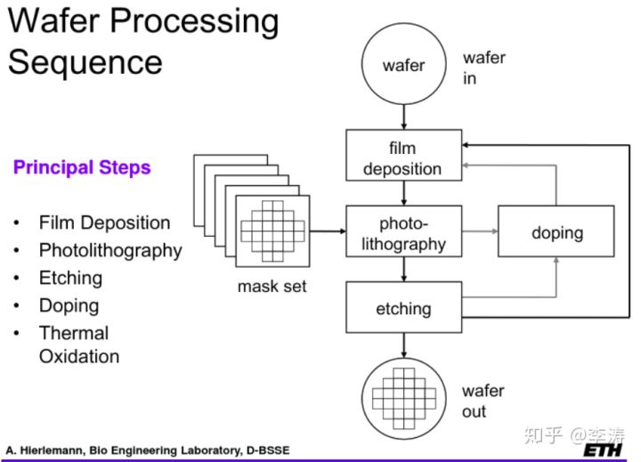
The process flow of a wafer, for example, involves a number of complex processing steps from the mask set to the actual wafer. Each process step can be abstracted as zi=Fi(xi,yi). xi is the input, yi is the process variant of the process and zi is the output. Because of the presence of each process step yi, the resulting wafer will have a certain probability of having failure points, or certain gates and alignment parameters deviating significantly from the design requirements, which can lead to functional problems with the chip.
What is semiconductor testing?
Traditionally, semiconductor test refers to product testing based on ATE machine, which is divided into wafer level CP test (chip probing) or FE test (FrontEnd test) and FT test (final test) or BE test (backend test) after packaging. Of course, with the promotion of WLCSP (wafer level chip scale package) package, more and more products only need CP test and then can be cut and delivered in pieces.
Traditional semiconductor testing is highly dependent on DFT design, a complete DFT design can provide high fault coverage test incentives to ensure that semiconductor testing can be used to minimize the time cost of screening out faulty chips. However, with the increase in chip hardware and software complexity, many problems can not or difficult to abstract the corresponding failure model, so SLT (system level test) is also used by most companies, placed in the FT test after the entire FT test fault coverage, to ensure that DPM (defects per million) to meet customer needs.
Why semiconductor testing is necessary?
The chip has a complete verification process in the design phase, simulation verification, UVM, formal verification and FPGA-based SLE (system level emulation) and other verification means to ensure 100% design functional correctness. Generally speaking, the chip can be flowed, and the netlist of the chip is verified by all test cases, and the design requirements are perfectly realized. So many people will wonder why every chip needs to go through the time and effort of rigorous semiconductor testing before it can be provided to customers?
Take the process flow of wafer as an example, from mask set to the real wafer, it needs to go through many complex processing steps. Each processing step can be abstracted as zi=Fi(xi,yi). xi is the input, yi is the process variant of the process, and zi is the output. Because of the existence of each processing step yi, the final chip on the wafer will have a certain probability of failure points, or some gates and some parameters of the alignment deviate seriously from the design requirements, which will lead to chip function problems.
In the mature 28nm process, for example, the overall yield is around 93% (wafer yield is generally around 93% while the yield after packaging is generally 99%). A complex electronic product such as a cell phone requires the integration of many chips on a substrate, the DPM of the whole system is the DPM product of each chip, so the DPM of each chip needs to be controlled below 500 to ensure that the integrator can produce qualified and reliable electronic products at low cost. In order to achieve the DPM target, semiconductor testing is the indispensable step to ensure the quality of the chips shipped. As the semiconductor process continues to probe down 1nm, the overall yield of the mass production process has also dropped to about 80%, more product production failure rate further requires more complete semiconductor test, otherwise low fault coverage of the test will lead to a large number of customer return, affecting the time to market of the product mass production.
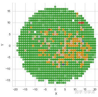
Semiconductor test data results are also used in process monitoring and optimization as well as product design optimization. For example, scan/mbist test will generally store the specific information of the failure in the database, a large number of product testing of these failure information will be back-labeled to wafer specific die, or even back-labeled to the layout of the X / Y coordinates, if there is an obvious defect signature appears, the process and design will need to check whether there is anything to cause this generic problem, whether there is room for improvement. Whether there is a place to improve.
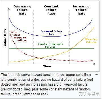
Semiconductor testing also uses stress to accelerate the aging test to reduce or avoid burn-in. burn-in generally takes 125C/24h, the purpose is to screen out early failing DUTs by stress according to the bath tub curve. Because the burn-in time is generally long, most products include ultra-high voltage short-time stress test in the ATE test can accelerate aging, with the shortest stress time to quickly screen out early failure DUTs.
Chip according to different applications, Jedec (Home | JEDEC) will have different qualification requirements, general qualification including ESD/latchup, HTOL, TC, ELFR, HTS, THB, etc.. Regardless of which qualification, before stress to use the complete ATE test procedures to screen out intact chips, after stress need to use the same procedures to do readout to determine whether the chip is damaged after stress. Therefore, for qualification, ATE testing is also indispensable and requires cooperation with test engineers in the project to develop a feasible plan.
Semiconductor test flow
For example, there are 5 test insertions in the test flow of automotive electronics, so many test insertions because the DPM of automotive electronics requires zero defect, and must be tested under different temperatures for many times to maximize The maximum number of tests at different temperatures to screen new products.

And generally used in consumer categories such as cell phone communication chips, because it does not involve life and public safety, DPM requirements are generally around 500,so the test process is also as simple as possible to reduce the cost of testing.
As shown in the figure below, the test temperature of wafer and device is determined according to the impact of the process on the logic/sram at different temperatures.
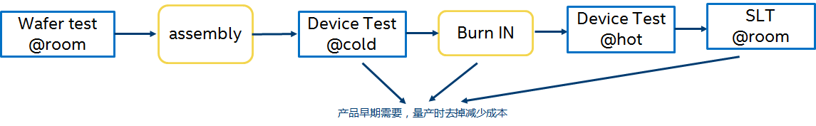
Because adding a test insertion, the test cost will increase significantly and the product profit will be reduced. Therefore an important task in semiconductor testing is to study how to achieve the same DPM target with as few test insertions as possible. In the above figure, for example, the goal was set early in the project that "the mass production program needs to remove device test@cold, burn-in, and SLT", and during the early test program development process, it was necessary to study how to try to add more tests to the retained test insertion (e.g. scan/mbist/IO stress tests, stricter pass/fail limits, etc.) in order to filter out the same problematic chips.
How to define the test content of different test insertion? In summary, test engineers need to be based on the probability of failure, test time and test conditions based on a comprehensive assessment.
The wafer test uses probe card + probe to realize the electrical connection between the chip and ATE machine, generally speaking, the contact resistance and inductive resistance value of the probe card is large, try to avoid the test frequency of high test (limited to 50M~100M), and focus on the scan/mbist and other tests with high failure rate, to ensure that more than 90% of the defects can be screened out at the wafer level without wasting time. wafer level sieve out without wasting the cost of assembly and FT testing.
FT testing generally need to implement all the tests in the early stages to ensure test coverage. In addition to screening defects, FT tests generally need to trim some analog modules such as bandgap, reference current, reference resistance, etc., as well as some other tests that require the results to be written to the fuse.
SLT generally uses a mini-system similar to the system application board to execute the system application software to filter out the defects that cannot be characterized by the failure model of DFT, or some performance-related functional tests that are limited by the ATE machine. However, because SLT testing does not easily provide specific data needed for process and design improvement, it is generally necessary to improve the fault coverage and effectiveness of ATE testing during mass production to minimize the number of defect devices entering SLT testing, with the ultimate goal of removing SLT testing.