


3-nanometer chip test success, foreign media: the rise of China's core


A Chinese chip company said their test of 3nm chip has been successful, showing that the domestic chip is not afraid of difficulties and dangers, and actively seize the existing chip foundation, the first breakthroughs have the opportunity to promote the technology, and ultimately realize the breakthrough from the point to the surface breakthrough.
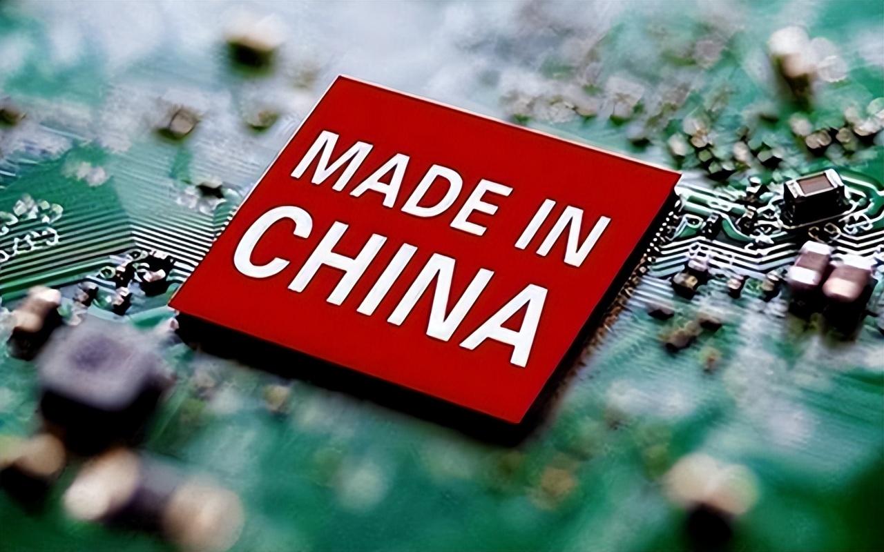
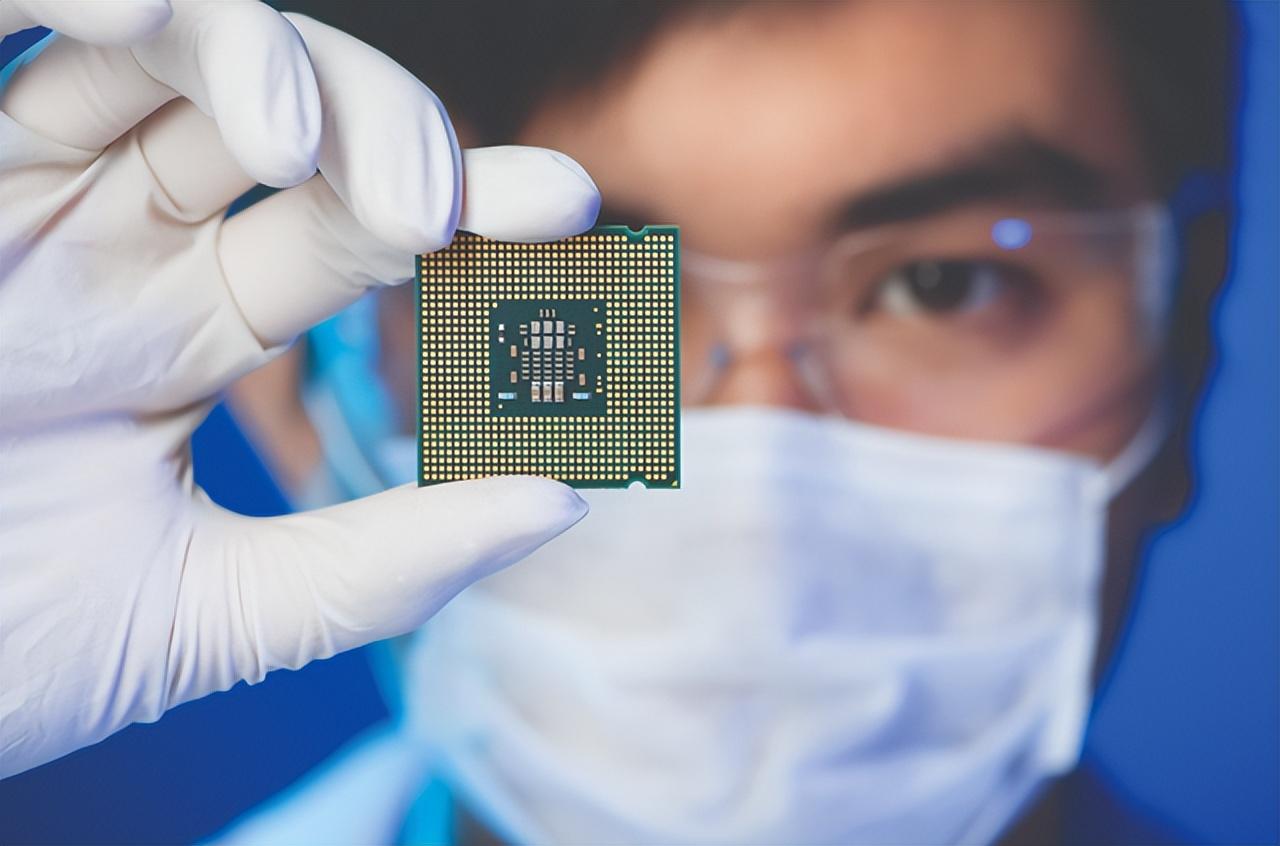
It is reported that Guangdong Liyang company has successfully realized 3 nm chip packaging test, which is another major breakthrough in domestic chips, packaging test technology has become the fastest progress of China's chip industry chain, the rise of China's chips has opened an important channel.
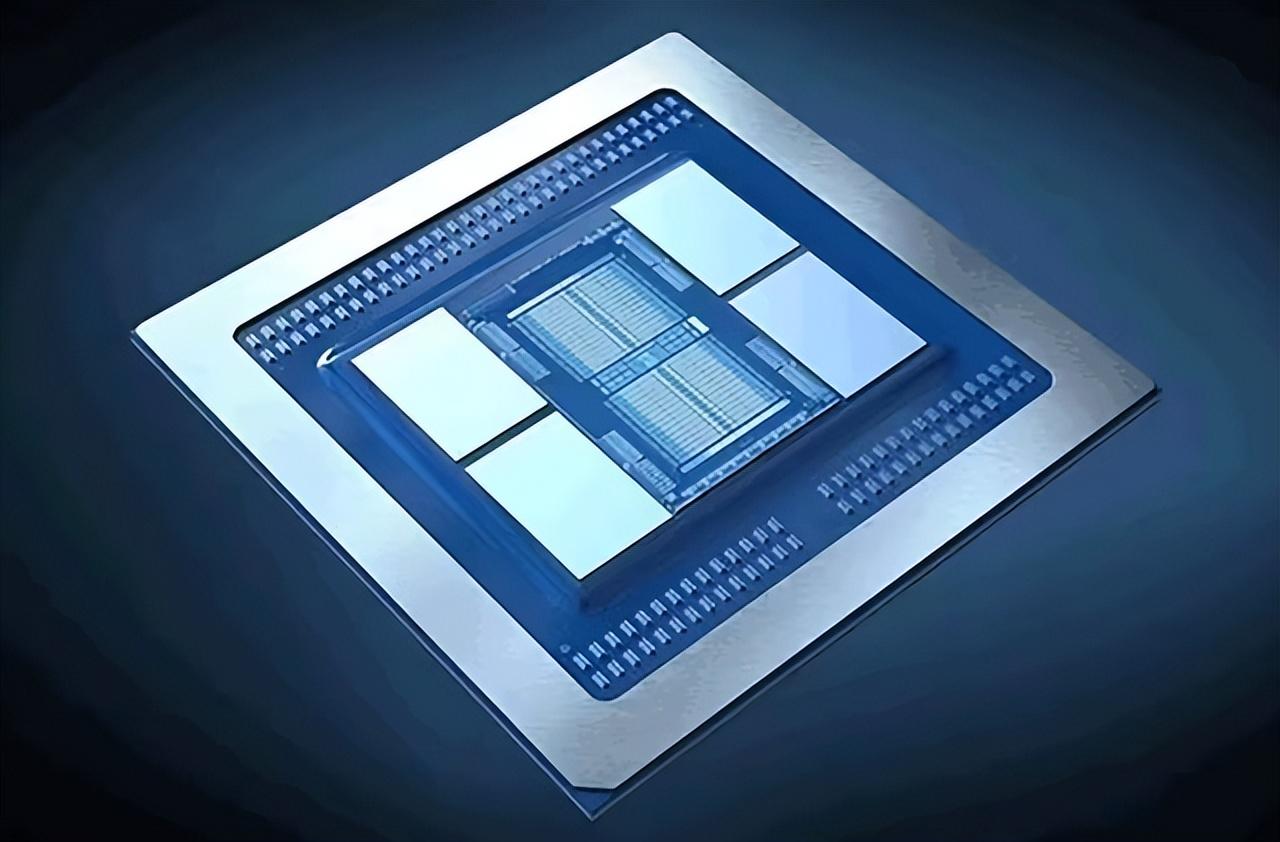
Chip packaging is an important part of chip manufacturing, it will be a chip from the chip manufacturing plant manufacturing wafer split into a chip, and will be a good chip to pick out, connected to the external circuitry and chip protection shell, become a chip we see in our daily lives, such as the CPU and other chips to see the appearance of the chip.
Chip packaging is very important, after all, after each wafer production is not every chip is available, for example, TSMC's current 3-nanometer process yield is only 55%, of which 45% for the useless chip, chip sealing and testing companies is the useless chip removed, and will be useful to pick out the chip and packaging.
China in the chip packaging has been at the forefront of the world, the world's top ten chip packaging companies, the United States is only one left, the other is the Asian region, three in mainland China, China Taiwan's packaging companies occupy most of the remaining position, it can be said that the United States of America's chip manufacturing and packaging now have been handed over to the Asian enterprises.
Guangdong Liyang company achieved 3 nm packaging technology to the overseas media marveled, they did not expect China's chips in such an environment can still make significant technological breakthroughs, so they have thought that China's chips are on the rise, can not stop China's chip in the footsteps of progress.
Chip production includes many links, according to industry sources pointed out that the production of chips can be roughly divided into eight links, in addition to the above chip packaging, China in the chip manufacturing and etching machine has reached 5 nanometers, in addition to several other links in addition to photolithography have reached 14 nanometers.
The United States tried to use their monopoly on EDA tools to stop China's chip, China's leading technology companies Huawei and domestic EDA companies to cooperate, the realization of the 14-nanometer and above process are used completely self-developed EDA tools, so that the United States plans to be thwarted, these are all indicative of the resilience of China's chip in various industries, the tougher the more is to show a strong potential.
As for the toughest link - lithography, China is also accelerating the advancement of earlier authoritative media reports pointed out that China's 28-nanometer lithography as soon as the end of the year before mass production, 28-nanometer lithography using immersion lithography technology, this lithography technology can be extended to 7 nanometers, once the 28-nanometer lithography into production, then China's photolithography will be accelerating the advancement of the 7-nanometer.
It can be said that China's major breakthrough in 3 nm packaging technology, the Chinese chip industry is of great significance, which shows that China's chip powerful innovation, even if there is a lot of resistance can not stop China's chip according to the existing technological base to achieve point breakthroughs, which is the aspect of the foreign media marveled at, and I believe that China's chip will be in the near future to achieve the full autonomy of the manufacture of advanced chips.
A Chinese chip company said their test of 3nm chip has been successful, showing that the domestic chip is not afraid of difficulties and dangers, and actively seize the existing chip foundation, the first breakthroughs have the opportunity to promote the technology, and ultimately realize the breakthrough from the point to the surface breakthrough.
It is reported that Guangdong Liyang company has successfully realized 3 nm chip packaging test, which is another major breakthrough in domestic chips, packaging test technology has become the fastest progress of China's chip industry chain, the rise of China's chips has opened an important channel.
Chip packaging is an important part of chip manufacturing, it will be a chip from the chip manufacturing plant manufacturing wafer split into a chip, and will be a good chip to pick out, connected to the external circuitry and chip protection shell, become a chip we see in our daily lives, such as the CPU and other chips to see the appearance of the chip.
Chip packaging is very important, after all, after each wafer production is not every chip is available, for example, TSMC's current 3-nanometer process yield is only 55%, of which 45% for the useless chip, chip sealing and testing companies is the useless chip removed, and will be useful to pick out the chip and packaging.
China in the chip packaging has been at the forefront of the world, the world's top ten chip packaging companies, the United States is only one left, the other is the Asian region, three in mainland China, China Taiwan's packaging companies occupy most of the remaining position, it can be said that the United States of America's chip manufacturing and packaging now have been handed over to the Asian enterprises.
Guangdong Liyang company achieved 3 nm packaging technology to the overseas media marveled, they did not expect China's chips in such an environment can still make significant technological breakthroughs, so they have thought that China's chips are on the rise, can not stop China's chip in the footsteps of progress.
Chip production includes many links, according to industry sources pointed out that the production of chips can be roughly divided into eight links, in addition to the above chip packaging, China in the chip manufacturing and etching machine has reached 5 nanometers, in addition to several other links in addition to photolithography have reached 14 nanometers.
The United States tried to use their monopoly on EDA tools to stop China's chip, China's leading technology companies Huawei and domestic EDA companies to cooperate, the realization of the 14-nanometer and above process are used completely self-developed EDA tools, so that the United States plans to be thwarted, these are all indicative of the resilience of China's chip in various industries, the tougher the more is to show a strong potential.
As for the toughest link - lithography, China is also accelerating the advancement of earlier authoritative media reports pointed out that China's 28-nanometer lithography as soon as the end of the year before mass production, 28-nanometer lithography using immersion lithography technology, this lithography technology can be extended to 7 nanometers, once the 28-nanometer lithography into production, then China's photolithography will be accelerating the advancement of the 7-nanometer.
It can be said that China's major breakthrough in 3 nm packaging technology, the Chinese chip industry is of great significance, which shows that China's chip powerful innovation, even if there is a lot of resistance can not stop China's chip according to the existing technological base to achieve point breakthroughs, which is the aspect of the foreign media marveled at, and I believe that China's chip will be in the near future to achieve the full autonomy of the manufacture of advanced chips.